
www.ptreview.co.uk
10
'26
Written on Modified on
Top-Side Cooling Semiconductor Packages for SiC MOSFETs
ROHM develops a surface-mount package architecture designed to maximize thermal dissipation and high-voltage insulation in automotive and industrial power conversion systems.
www.rohm.com
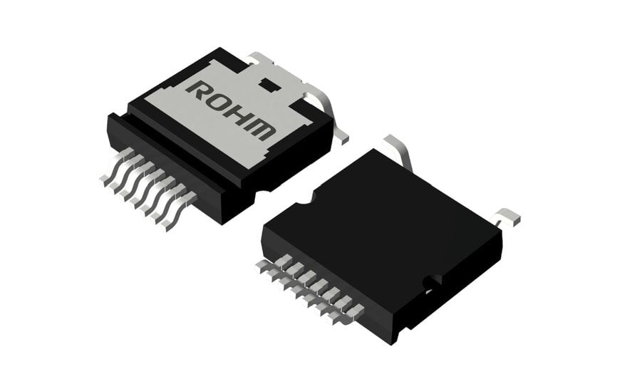
ROHM has released a top-side cooling package for silicon carbide (SiC) MOSFETs to enable automated surface-mount assembly while maintaining thermal performance equivalent to conventional through-hole components. This packaging technology addresses the high thermal density and isolation requirements found in electric vehicle onboard chargers, electric compressors, photovoltaic inverters, and high-performance industrial server power supplies.
Thermal Dissipation and Manufacturing Automation
High-power density conversion circuits traditionally utilize through-hole packages, such as the TO-247-4L, due to their large internal copper leadframes and direct mounting to external heatsinks. However, through-hole integration requires manual wave soldering or secondary selective soldering steps, which limits production throughput.
The top-side cooling architecture shifts the primary thermal interface to the upper surface of the component. This allows the printed circuit board (PCB) to remain dedicated to signal routing and electrical traces, while an isolated heatsink can be clamped directly over the top of the package. By separating the thermal path from the PCB layer, the design eliminates the need for thermal vias and thick copper internal planes, reducing overall system profile and facilitating full compatibility with standard surface-mount automated assembly lines.
High-Voltage Creepage and Insulation Geometry
Operating in higher-voltage environments, such as 800 V automotive traction networks, introduces stringent safety requirements regarding electrical creepage—the shortest distance along the surface of an insulating material between two conductive parts.
The package incorporates a proprietary surface groove structure that establishes a continuous creepage distance of 6.66 mm. This physical dimension permits a maximum working AC peak voltage of 1200 V under Pollution Degree 2 conditions (environments where only non-conductive pollution occurs, except for occasional temporary conductivity caused by condensation). This integration enables space-constrained system designs without necessitating secondary conformal coating or manual potting steps to pass regulatory high-voltage isolation clearances.
Power Conversion Efficiency and Semiconductor Performance
The implementation utilizes fourth-generation silicon carbide trench MOSFET structures inside the package enclosure to minimize both static and dynamic losses. By combining low drainage-source on-resistance (RDS(on)) with minimized parasitic gate capacitance, the internal chips accelerate turn-on and turn-off transitions.
This reduction in total switching energy (Eon and Eoff) allows the power conversion circuits to operate at higher switching frequencies. Increasing the frequency directly diminishes the required volumetric size and weight of associated passive components, such as power inductors and DC-link capacitors, maximizing the power density within the digital supply chain. The component line was detailed at the PCIM 2026 trade exposition in Nuremberg, Germany, held from June 9 to June 11, 2026.
Additional Context
This section details technical specifications and competitive benchmarking not included in the original news release.
The top-side cooling surface-mount design targets an industry segment currently addressed by established packages, notably the Toll (Transistor Outline Leadless) package and the QDPAK (Quarter DPAK) configuration used by competitors like Infineon Technologies and STMicroelectronics. Standard Toll packages maximize PCB contact area but rely on bottom-side cooling, which injects heat directly into the circuit board substrate, limiting total power dissipation to the thermal capacity of the copper layout.
Comparatively, the 6.66 mm creepage clearance of the TSC3PAK matches or exceeds the standard 6.1 mm clearance found in conventional QDPAK architectures. This provides a safety margin against voltage tracking or arcing across the package pins under high-voltage transients. The physical envelope dimensions (14.00 × 18.58 × 3.50mm) provide a thermal junction-to-case resistance (Rth(j-c)) that aligns with through-hole equivalents, allowing power designers to transition to automated pick-and-place lines without modifying the core thermal management hardware of the cooling system loop.
Edited by Aishwarya Mambet, Induportals Editor, with AI assistance.
www.rohm.com
